 | ÐлекÑÑоннÑй компоненÑ: FQP7N60 | СкаÑаÑÑ:  PDF PDF  ZIP ZIP |
Äîêóìåíòàöèÿ è îïèñàíèÿ www.docs.chipfind.ru

Rev D, July 2000
July, 2000
1
AN9008
The Use of QFETs in a Flyback Converter
By Il Soo Yang
Introduction
Power supply designers face many challenges in designing more efficient and cost-effective power
supplies. Efficiency is a major consideration in designing switching power supplies. Many factors in
the design process such as the input filter capacitance, transformer core geometry and construc-
tion, output rectifier, and switching device etc., affect the efficiency of switching power supplies.
Among the losses all components generate, switching device losses occupy about 30%. Hence,
selecting MOSFETs with optimum efficiency and high reliability is very crucial in power supply
design. This application note compares the key characteristics, power losses, and efficiency of the
new QFET and a conventional MOSFET in a 60 watt flyback converter operated at 180 to 265
VAC.
QFET Characteristics
Almost all the power supplies used in TVs, VCRs, PCs, fax machines, and other home appliances
rely on a switching circuit to convert the AC wall power to DC power or DC to AC. Thus, they are
referred to as switched mode power supplies. To obtain high efficiency, it is crucial for designers to
select switching MOSFETs to give very low losses in the circuits. MOSFETs must exhibit low con-
duction and switching losses with safety qualifications. Fairchild Semiconductor, in extending its
commitment to develop high quality MOSFETs, now offers new high efficiency QFETs for switched
mode power supply applications.
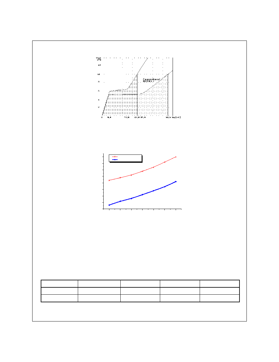
A power QFET, rated at 600V and used in a 60 watt flyback converter, features a gate charge rat-
ing which is 45 percent lower than existing devices for improved switching and drive efficiency. Fig-
ure 1 compares the new QFET FQP7N60 with its conventional MOSFET counterpart. By using
unified singular well stripe technology, the Miller capacitance of the new QFET is reduced by about
40 percent.
2
Rev D, July 2000
:
Figure 1: Gate Charge Improvement
Balanced with gate charge improvement, the on-resistance [R
ds(on)
] goes down by about 20 per-
cent with respect to previous devices versus drain current. Figure 2 shows the improvement of on-
resistance in a QFET compared with a MOSFET.
Figure 2: On-resistance Improvement vs. Drain Current
The combined improvement of gate charge and on-resistance in this 60 watt flyback converter
leads to a more efficient system because of the reduced turn-off conduction loss. It is worth
emphasizing that QFETs offer designers significant improvements in terms of lower overall system
cost due to lower gate driver requirements, a smaller heat sink, and narrower PCB. Table 1 illus-
trates the features which are useful in flyback converters and other applications.
Table 1: Q
g
and R
ds(on)
Improvements
Voltage Rating
Device
On-resistance
Gate Charge
Package
600V
Conventional Part
1.2
65 nC
TO-220
600V
FQP7N60(QFET) 1.0
38 nC
TO-220
Q F E T
F Q P 7 N 6 0
1
2
3
4
5
6
7
0.70
0.75
0.80
0.85
0.90
0.95
1.00
1.05
1.10
Conventional MOSFET
QFET (FQP7N60)
O
n
-
R
es
i
s
t
a
nc
e :
R
d
s
(
on)
[
]
Drain Current : Id [A]
3
Rev D, July 2000
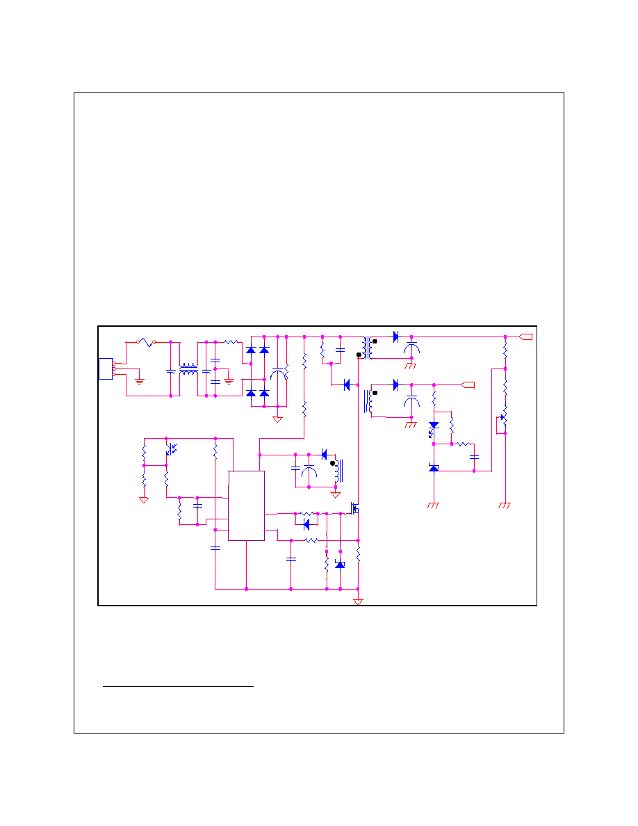
Performance in a Flyback Converter
Figure 3 shows the design of a commercially available 60 watt flyback converter with two outputs
(+160V, +15V), operating at a switching frequency of 80kHz and an input voltage of 220VAC. This
type of switching power supply is used for applications, such as monitors, TVs, and miscellaneous
instruments, requiring multiple output voltages . This discontinuous mode flyback converter, using
a KA3882 current mode controller, features good voltage tracking with the use of pulse by pulse
current sensing on the primary side, and an isolated secondary feedback loop. The PWM IC
KA3882 directly drives the power MOSFET.
As the power MOSFET sequentially turns on and off, energy is stored in the transformer core dur-
ing the on time, and is then transferred to the output capacitor during the off time. When the power
MOSFET turns off, the energy stored in the leakage inductance causes a voltage spike across the
drain-to-source terminal of the power MOSFET, which amounts to at least twice the input voltage
(Vin + nVo + leakage inductance voltage
1
). Most applications need clamp circuits to restrict this
voltage spike from exceeding the BVdss rating of a MOSFET. A power MOSFET must have high
voltage capability with lower on-resistance and smaller gate charge for higher efficiency.
Figure 3: Flyback Converter Circuit Diagram
1. 'n' indicates a turns ratio of the transformer windings. The voltage of Vin + nVo + leakage inductance voltage of the transformer appears at
the primary side.
7
8
6
3
5
2
1
4
KA3882
L1
D1
T1
Fuse
U1
U2
U3
Q1
Vout1
Vout2
QFET(FQP7N60)
or Conventional
MOSFET
Vin=220VAC
1
2
3
C1
1
2
1
2
C4
1
2
1
2
1
5
4
8
C2
1
2
C3
1
2
C5
1
2
R2
1
2
1
2
1
2
1
2
R1
1
2
R3
1
2
1
2
3
R5
1
2
C6
1
2
R14
1
2
1
2
D3
1
2
C10
1
2
C9
1
2
R11
1
2
D4
1
2
R11
1
2
R13
1
2
D5
1
2
C8
1
2
R10
1
2
1
3
C7
1
2
R9
1
2
R6
1
2
R7
1
2
R8
1
2
R19
1
2
R20
1
3
2
1
2
D7
1
2
C13
1
2
R14
1
2
R16
1
2
R17
1
2
1
2
1
2
C14
1
2
D2
1
2
C11
1
2
R4
1
2
C12
1
2
R18
1
2
1
5
4
8
D6
1
2
5V 0.8A
160V 0.3A
4
Rev D, July 2000
Table 2: Power Supply Specifications
This flyback converter was tested in rated conditions of 220VAC input voltage, 80kHz switching
frequency, and 60W output power.
Figure 4 shows the waveforms for rated operating conditions using the QFET(FQP7N60) as the
switching device. The QFET is driven by a gate-source voltage of 15V and the voltage spike
across the drain-source terminal is adequately clamped to about 500V by an additional clamp cir-
cuit during off-time.
Figure 4: Operating Waveforms at Rated Conditions (V
in
=220VAC, P
out
=60W)
1. Operating mode
:
Flyback Discontinuous Mode
2. Input voltage (V
in
)
:
180 VAC to 265 VAC (50Hz/60Hz)
3. Switching frequency (f
sw
)
:
80 kHz
4. Output voltage (V
out
)
:
A. 160V ± 5% 0.3A
B. 15V ± 5% 0.8A
5. Efficiency (
)
:
75%
Vgs(5V.div)
Id(1A/div)
Vds(250V/div)
5
Rev D, July 2000
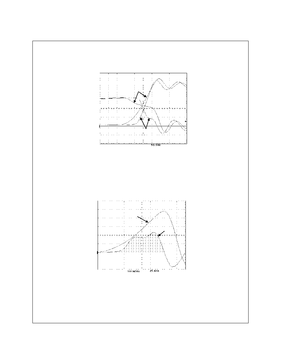
Figure 5 compares the waveforms of a conventional MOSFET with the new QFET(FQP7N60) at
turn-off without the additional clamped circuit (R5, C6, and D2), and the high conduction diode (D4)
for gate discharging (refer to Figure 3).
Figure 5: Turn-off Improvement at Rated Conditions (V
in
=220VAC, P
out
=60W)
Note that the switching time of the QFET is faster than that of the conventional MOSFET because
of the reduction of gate charge by at least 45 percent. Figure 6 shows the difference in turn-off loss
between both MOSFETs without clamped circuits and the conduction diode, D4. The turn-on loss
in the crossover losses is very small and can be negligible. The turn-off loss period is due to the
finite switching time of the MOSFET which is directly related to the gate charge.
Figure 6: Turn-off Loss Improvement
Conventional
MOSFET
QFET
Id(0.5A/div)
Vds(100V/div)
/div
Conventional
MOSFET
QFET
/div